
Home
People
Research
Publication
News
Link
Large-Area
3-D Nano-Patterning and Nanostructure Fabrication
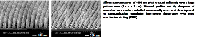
As scientific quests and engineering
applications reach down to a nanometer scale, there is a strong need to
fabricate nanostructures with good regularity and controllability of their
pattern, size, and shape. In many applications, furthermore, the nanostructures
are not useful unless they cover a relatively large area and the manufacturing
cost is within an acceptable range. While several nanoscale patterning
techniques are available, it should be noted that serial lithography methods do
not cover a large area needed for non-electronic applications. Other
non-lithographic methods, for example, the use of nanotemplates
or the direct growth of nanoscale structures do not provide good regularity over
a large area. One of our research interests is to develop a simple but efficient
nanofabrication method with superior control of pattern regularity, size, and
shape over a large area, which will open new application possibilities in many
scientific and engineering domains.
References
1.
I.
Wathuthanthri, C.-H. Choi, “Tunable Lloyd-Mirror Interferometer
for Large-Area Nanopatterning”, in Proceedings of ASME IMECE, November 15-19, 2009, Orlando,
FL, USA.
2.
C.-H.
Choi, C.-J. Kim,
“Design, Fabrication, and Applications of Large-Area Well-Ordered
Dense-Array Three-Dimensional Nanostructures”, in Nanostructures in
Electronics and Photonics, Ed. Faiz Rahman, Pan Stanford Publishing (2008)
(invited).
3.
C.-H. Choi, C.-J. Kim, “Fabrication of Dense
Array of Tall Nanostructures over a Large Sample Area with Sidewall Profile and
Tip Sharpness Control”, Nanotechnology
17, 5326-5333
(2006).
Nanoscale
Interfacial Phenomena
Fundamental scientific quests, which were
unexplored before due to the lack of experimental precision, can now be explored
with the recent development of nanotechnology. Especially, various interfacial
phenomena at nanoscale can now be explored by using well-tailored
nanomechanical properties of nanostructures. One of our research interests is to investigate the nanoscale
interfacial phenomena including
friction, adhesion, and fluid/thermal transport phenomena.
References
Interfacial
liquid slip:
1.
C. Lee, C.-H. Choi, C.-J. Kim, “Structured
Surfaces for a Giant Liquid Slip”, Physical Review Letters 101, 064501 (2008).
2.
C.-H. Choi, C.-J. Kim, “Large
Slip of Aqueous Liquid Flow over a Nanoengineered Superhydrophobic Surface”,
Physical Review Letters 96, 066001 (2006).
3.
C.-H. Choi, U. Ulmanella, J. Kim, C.-M. Ho,
C.-J. Kim, “Effective
Slip and Friction Reduction in Nanograted Superhydrophobic
Microchannels”, Physics of Fluids 18, 087105 (2006)
4.
C.-H. Choi, K. J. A.
Westin, K. S. Breuer, “Apparent
Slip Flows in Hydrophilic and Hydrophobic Microchannels”, Physics
of Fluids 15, 2897-2902 (2003).
Cell adhesion:
1.
C.-H. Choi, S. H. Hagvall, B. M. Wu, J. C. Y.
Dunn, R. E. Beygui, C.-J. Kim, “Cell
Growth as a Sheet on Three-Dimensional Sharp-Tip Nanostructures”, Journal of Biomedical Materials Research 89A, 804-817 (2009).
2.
S. Heydarkhan-Hagvall, C.-H. Choi, J. Dunn, S. Heydarkhan, K.
Schenke-Layland, W. R. MacLellan, R. E. Beygui, “Influence
of Systematically Varied Nano-Scale Topography on Cell Morphology and Adhesion”,
Cell Communication & Adhesion 14, 181-194 (2007).
3.
C.-H. Choi, S. H. Hagvall, B. M. Wu, J. C. Y.
Dunn, R. E. Beygui, C.-J. Kim, “Cell
Interaction with Three-Dimensional Sharp-Tip Nanotopography”,
Biomaterials 28, 1672-1679 (2007).
Droplet
evaporation kinetics and wetting dynamics:
1.
R. Leeladhar, W.
Xu, C.-H. Choi, “Effects of Nanofluids on Droplet Evaporation and
Wetting on Nanoporous Superhydrophobic
Surfaces”, in Proceedings of ASME MNHMT, December 18-22, 2009, Shanghai,
China.
2.
W. Xu, C.-H.
Choi, “Effects of Structural Topography on Nanofluids Droplet
Evaporation on Multifarious Superhydrophobic Surfaces”, in Proceedings of
ASME MNHMT, December
18-22, 2009, Shanghai, China.
3.
C.-H. Choi, C.-J. Kim, “Droplet Evaporation of
Pure Water and Protein Solution on Nanostructured Superhydrophobic Surfaces of
Varying Heights”, Langmuir 25, 7561-7567 (2009).
Multifunctional
Superhydrophobic Surfaces
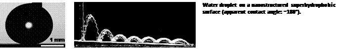
Nature such as plants, insects,
and marine animals uses micro- and nano-textured
surfaces in their components (e.g., leaves, wings, eyes, legs, and skins) for
multi-purposes such as self-cleanness. Such multi-functional surface properties
are attributed to the 3-D surface structures. Especially, hydrophobic surface
structures create a composite interface with liquid by retaining air between
the structures, minimizing the contact area with liquid. Such non-wetting
surface property, so-called superhydrophobicity, can
offer numerous application potentials including anti-fogging, anti-snow
adhesion, anti-frosting, anti-corrosion, low flow-friction, and
anti-biofouling. One
of our research interests is to develop
multi-functional superhydrophobic surfaces of optimized de-wetting stability
and adaptive self-healing capability for various applications.
References
1.
C.-H. Choi, C.-J. Kim,
“Nanostructured surfaces for anti-biofouling/anti-microbial
applications”, in Proceedings of the SPIE Defense, Security, and Sensing, April 13-17, 2009, Orlando, FL,
USA.
2.
C.-H. Choi, C.-J. Kim, “Large
Slip of Aqueous Liquid Flow over a Nanoengineered Superhydrophobic Surface”,
Physical Review Letters 96, 066001 (2006).
3.
C.-H. Choi, U. Ulmanella, J. Kim, C.-M. Ho,
C.-J. Kim, “Effective
Slip and Friction Reduction in Nanograted
Superhydrophobic Microchannels”, Physics of Fluids 18,
087105 (2006).
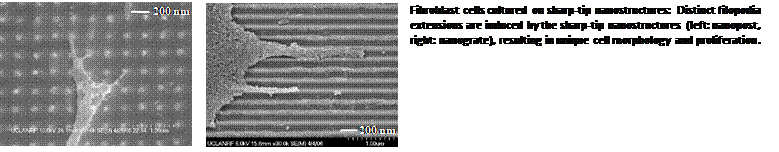
Microfluidic
Self-Assembly of Nanomaterials
Nanomaterials are promising building
blocks for novel nanostructures and nanodevices. However, practical
applications require precise arrangement of nanomaterials into hierarchical
orders to construct desired geometry with controllable shape, location and
direction on
a large scale. Although several
strategies had been explored for the controlled placement of nanoscale building
blocks, the
development of more efficient techniques is still essential to achieve
well-ordered high-throughput nanoassembly. One of our
research interests is to develop a simple
and efficient nanoassembly mechanism based on various
microfluidic techniques to result in site-specific self-assembly of
nanomaterials.
References
1.
R. Leeladhar, W.
Xu, Y.-T. Tsai, E.-H. Yang, C.-H. Choi, “Nanowire Self-Assembly in
Droplet Evaporation on Superhydrophobic Surfaces”, in Proceedings of
the 13th International Conference on
Miniaturized Systems for Chemistry and Life Sciences (MicroTAS 2009), November 1-5, 2009, Jeju, Korea.
2.
Y.-T. Tsai, W.
Xu, E.-H. Yang, C.-H. Choi, “Interfacial-Tension-Directed
Self-Assembly of Nanowires on a Superhydrophobic Surface”, in Proceedings of
ASME IMECE, November
2-6, 2008, Boston, MA, USA.
Nanofluidic
Energy Harvesting
This project is to develop a
novel power generation device, utilizing a nanofluidic platform containing nanoenergetic materials, which are extremely mass-efficient
in storing chemical energy. The stored chemical energy can be released rapidly,
generating heat and pressure as a stimulus exists. These released energies need
to be transformed to electricity and ultimately stored in energy storage
devices, which can be used to power sensors, switches and fuzes.
The technology will transform the energy created by energetic materials into
electrical energy by using a nanofluidic system.
Optofluidic
Waveguides and Sensors
Most optical systems are made with solid materials such as glasses,
metals, and semiconductors. However, there are cases in which it will be
advantageous to use fluids for optical systems. Whereas microfluidics has made
it possible to integrate multiple fluidic tasks on a chip, most optical
components, such as the light source, sensors, lenses, and waveguides, remained
off the chip. In recent development of optofluidic integration, optics and
microfluidics are combined on the same chip by building the optics out of the
same fluidic toolkit. The advantage of optofluidics
lies in the ease with which one can change the optical properties of the
devices by manipulating fluids. The project is to study and develop new
optofluidic waveguide architecture of liquid-core and air-cladding for
multi-phase (liquid and gas) sensing with greater sensing efficiency.
Home
People
Research
Publication
News
Link
©2007 Nature Inspired Surface
Engineering (NISE) Laboratory