Scalable INtegrated Electronics Laboratory
Stevens Institute of Technology
Home
News
Team
Projects
Publication
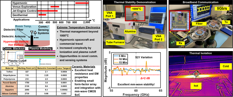
High-Temperature mm-Wave/THz Fibers
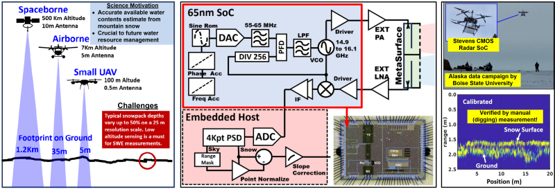
Snow Sensing CMOS Radar